ADC Explained: Resolution, Reference Voltage, and ESP32 Limits

Push button wired to an Arduino input pin with a 10k pull-up resistor

ADC Explained: Resolution, Reference Voltage, and ESP32 Limits

An ADC, or analog to digital converter, turns a voltage into a number. A 12-bit ADC divides its input range into 4,096 steps, numbered 0 to 4,095. A 10-bit ADC divides the range into 1,024 steps, numbered 0 to 1,023. The reference voltage sets the top of that range, and on the ESP32 ADC2 pins stop working while Wi-Fi runs.

ADC explained: what is an ADC?

An ADC measures a voltage on a pin and returns a digital number. The number is proportional to the input voltage divided by the reference voltage, times the number of steps. A sensor that outputs a voltage, such as a temperature sensor, a light sensor or a potentiometer, needs an ADC to turn its signal into a number your code can use. A sensor that outputs a digital signal, such as an I2C temperature sensor, does not need an ADC, because the sensor chip does the conversion itself.

Most microcontroller ADCs use successive approximation, or SAR. The ADC samples the pin voltage, compares it against an internal reference in a series of steps, and writes a digital value. The conversion takes microseconds, and the result is a single number per read. That number is not a voltage until your code converts it, using the resolution and the reference voltage.

What is resolution and why does it matter?

Resolution is the number of bits in the ADC result, and it decides the smallest voltage change the ADC can see. A 10-bit ADC has 1,024 steps. A 12-bit ADC has 4,096 steps. On a 3.3 V range, a 10-bit step is 3.3 V divided by 1,024, or about 3.22 mV per step. A 12-bit step is 3.3 V divided by 4,096, or about 0.81 mV per step. The 12-bit ADC sees a change four times smaller than the 10-bit ADC.

ADC resolution (bits) Steps (count) Step size on 3.3 V (mV) Boards
10 1,024 3.22 Arduino Uno, Nano, ESP8266
12 4,096 0.81 ESP32, ESP32-S3, Raspberry Pi Pico, RP2040

More bits do not always mean more accuracy. The ESP32 ADC is 12-bit, but its effective resolution is about 10 to 11 bits, because noise and nonlinearity eat the last bits. Averaging 16 to 64 readings gives a steadier result than chasing the last bit of a single read. A 10-bit ADC on an Arduino Uno with a clean supply and a short wire can beat a noisy 12-bit reading on a long wire next to a Wi-Fi antenna.

What is reference voltage?

The reference voltage is the voltage that maps to the top ADC value. On an Arduino Uno, the default reference is the 5 V supply, so a 5 V input reads 1,023 and a 2.5 V input reads about 511. On the Raspberry Pi Pico, the reference is 3.3 V, so a 3.3 V input reads 4,095. On the ESP32, the reference voltage is about 1.1 V at the ADC itself, not 3.3 V, and the chip applies attenuation to scale the input before it reaches the ADC.

That ESP32 detail causes the most confusion. A 3.3 V signal on an ESP32 ADC pin does not damage the pin, because the attenuation scales it down before the converter, but the raw reading does not map linearly to 3.3 V without the attenuation setting. Use analogReadMilliVolts on the ESP32 Arduino core, which applies the factory calibration and returns millivolts, instead of converting the raw count yourself with a 3.3 V assumption.

What is attenuation on the ESP32?

Attenuation reduces the input voltage before it reaches the ADC, which widens the measurable range. The ESP32 Arduino core offers four settings: 0 dB, 2.5 dB, 6 dB and 11 dB. At 0 dB, the measurable range is about 0 mV to 950 mV. At 2.5 dB, it is about 100 mV to 1,250 mV. At 6 dB, it is about 150 mV to 1,750 mV. At 11 dB, it is about 150 mV to 2,450 mV, which is the widest range and the default in the Arduino core.

Set the attenuation per pin for your sensor range. A sensor that outputs 0 V to 1 V needs 2.5 dB attenuation. A sensor that outputs 0 V to 3.3 V needs 11 dB attenuation, and even then the top of the range saturates at about 3.1 V. The ESP32 ADC is also nonlinear near the ends of its range, so readings near 0 mV and near the top are compressed. For a battery voltage measurement, use a voltage divider that keeps the ADC input in the middle of its range, and average many readings.

Why does ADC2 stop working with Wi-Fi on the ESP32?

The original ESP32 has two ADC units. ADC1 has 8 channels on GPIO 32 to 39. ADC2 has 10 channels on GPIO 0, 2, 4, 12 to 15 and 25 to 27. The Wi-Fi driver uses ADC2 internally, so ADC2 cannot be read while Wi-Fi is active. The Espressif ESP-IDF ADC guide states this directly: the application can only use ADC2 when the Wi-Fi driver has not started, and a read on ADC2 fails between Wi-Fi start and Wi-Fi stop.

The symptom is a sensor that reads correctly before WiFi.begin and returns zero or a stale value after the connection starts. The fix is to move the sensor to an ADC1 pin, GPIO 32 to 39. Remember that GPIO 34 to 39 are input only, so they read a sensor but cannot drive an output. The S3 also restricts ADC2 while Wi-Fi runs. The C3 has only one ADC unit, so it has no ADC2 conflict at all. Check the ADC section of your chip datasheet before you wire a sensor.

Some ADC2 pins carry extra traps. GPIO 0, 2 and 15 are strapping pins, so a sensor on those pins can stop the board from booting. On the ESP32 DevKitC, GPIO 0 cannot be used freely because of the auto program circuit. Prefer ADC1 pins for any sensor in a Wi-Fi project, and keep ADC2 for projects with no Wi-Fi at all.

How do Arduino, ESP32 and Pico ADCs compare?

Spec (unit) Arduino Uno ATmega328P ESP32 Raspberry Pi Pico RP2040
Resolution (bits) 10 12 12
Steps (count) 1,024 4,096 4,096
ADC channels (count) 6 on DIP, 8 on TQFP 18 across two units 4 external plus temperature
Reference voltage (V) 5, supply by default About 1.1 before attenuation 3.3
Max sample rate About 10 ksps Up to 2 Msps with DMA 500 ksps
Wi-Fi conflict None ADC2 blocked by Wi-Fi None on base Pico

The Pico ADC is the simplest to use: a 3.3 V reference, 12-bit resolution, and no Wi-Fi conflict on the base board. The Arduino ADC is the simplest to understand: a 5 V reference and a direct count to voltage conversion. The ESP32 ADC is the most capable and the most confusing, because of its attenuation settings and its ADC2 conflict, so read the ADC section of the ESP-IDF guide before you trust a reading.

How do you get an accurate reading?

Follow five steps. First, pick an ADC1 pin on the ESP32, or any ADC pin on the Pico or Arduino. Second, set the attenuation for your sensor range on the ESP32, or set the reference on the Arduino. Third, keep the wires short and add a 0.1 uF capacitor from the ADC pin to ground to filter noise. Fourth, average 16 to 64 readings instead of trusting one. Fifth, use the calibrated millivolt function where the core provides one, such as analogReadMilliVolts on the ESP32, instead of converting the raw count with an assumed reference.

Never exceed the ADC input voltage. On the ESP32, the pin tolerates 3.3 V, but the measurable range tops out near 3.1 V at 11 dB attenuation. On the Pico, the pin tolerates 3.3 V and the ADC input must stay below the 3.3 V supply plus a small margin. On the Arduino Uno, the pin tolerates 5 V. A sensor that outputs more than the ADC range needs a voltage divider, and the divider ratio must be included in your conversion math.

Code: read an ESP32 ADC pin with averaging

The sketch below reads an ESP32 ADC1 pin with 11 dB attenuation and averages 32 readings. It uses the ESP32 Arduino core. It was not compiled in this draft, and the compile result is logged as code not compiled in the header.

// ESP32 ADC read with averaging on an ADC1 pin
// Board: ESP32 DevKit V1. Sensor on GPIO 34, which is ADC1 channel 6.
const int adcPin = 34; // ADC1 only, so Wi-Fi can run at the same time

void setup() {
  Serial.begin(115200);
  analogSetPinAttenuation(adcPin, ADC_11db); // Widest range, about 0 to 3.1 V
  analogReadResolution(12); // 12-bit result, 0 to 4095
}

void loop() {
  long total = 0;
  for (int i = 0; i < 32; i++) {
    total += analogReadMilliVolts(adcPin); // Calibrated millivolts, not raw counts
    delay(2);
  }
  long averageMilliVolts = total / 32;
  Serial.print("Sensor voltage (mV): ");
  Serial.println(averageMilliVolts);
  delay(500);
}

For the Pico ADC pins in this guide, see the Raspberry Pi Pico pinout guide.

FAQ

Why does my ESP32 analogRead return 0 when Wi-Fi is on?

Your sensor is on an ADC2 pin, and the Wi-Fi driver uses ADC2. Move the sensor to an ADC1 pin, GPIO 32 to 39, and the readings return.

Is a 12-bit ADC always better than a 10-bit ADC?

No. A 12-bit ADC has finer steps, but noise and nonlinearity limit its effective resolution to about 10 to 11 bits on the ESP32. A clean 10-bit reading beats a noisy 12-bit reading, so average many samples and keep wires short.

What voltage can I put on an ESP32 ADC pin?

Up to 3.3 V on the pin. The measurable range tops out near 3.1 V at 11 dB attenuation, so a sensor above that needs a voltage divider.

How many ADC pins does the ESP32 have?

18 channels across two ADC units: 8 on ADC1 at GPIO 32 to 39, and 10 on ADC2 at GPIO 0, 2, 4, 12 to 15 and 25 to 27. A 30-pin board exposes 16 of them, because GPIO 37 and 38 are not broken out.

What is the ADC reference voltage on an Arduino Uno?

5 V by default, from the supply. A 5 V input reads 1,023 and a 2.5 V input reads about 511. The reference can be changed to the internal 1.1 V bandgap or an external AREF voltage.

Parts used

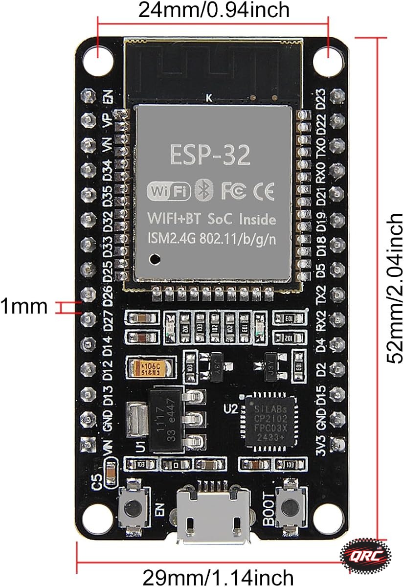
ESP32 DevKit V1 Development Board, 30-Pin WROOM-32: the ESP32 board for the ADC examples, with 18 ADC channels. ELEGOO UNO R3 Microcontroller Board: the Arduino board for the 10-bit ADC comparison.

Sources

Last updated: 2026-11-21. Search volume: not verified. Product links use the store short link form with the product ID; confirm the product slug at publish time.
How to Read a Microcontroller Datasheet: Specs That Matter

Microcontroller datasheet open beside an ESP32 board and a Raspberry Pi Pico

How to Read a Microcontroller Datasheet: Specs That Matter

Read a microcontroller datasheet in this order: absolute maximum ratings first, recommended operating conditions second, the pinout and pin function table third, and the electrical characteristics fourth. The single most important distinction is that absolute maximum ratings are stress limits that damage the chip when exceeded, while recommended operating conditions are the values the chip is guaranteed to work at.

Microcontroller datasheet: what is a datasheet and which document do you need?

A datasheet is the manufacturer document that defines a chip: its features, its pinout, its electrical limits, its timing and its package. It is the primary source for every spec in a project, and it outranks tutorials, forum posts and product listings. When two sources disagree, the datasheet wins.

Three documents are often confused. The chip datasheet covers the silicon, such as the ESP32 or the RP2040. The module datasheet covers the module built on that chip, such as the ESP32-WROOM-32, including its antenna and its flash. The board schematic and board guide cover the development board, such as the ESP32 DevKit V1 or the Raspberry Pi Pico, including which chip pins reach the header and which are used by the USB chip or the flash. Chip pins and board pins differ, so read the board document for wiring and the chip datasheet for limits.

Check the revision and the date on the first page. The Espressif ESP32 Series Datasheet is at version 5.3 in the copy checked for this post. The ESP32-C3 Series Datasheet is at version 2.5. The Raspberry Pi RP2040 Datasheet is at build date 2025-02-20, build version 3184e62-clean. The Microchip ATmega328P datasheet is DS40002061B. A revision changes pin functions, current limits and errata, so a tutorial written against an old revision can be wrong for the chip you hold.

What are absolute maximum ratings?

Absolute maximum ratings are the stress limits beyond which the chip can be damaged. They are not operating conditions, and the chip is not guaranteed to work at them. The ATmega328P datasheet, DS40002061B, lists the absolute maximum supply voltage as 6.0 V, the voltage on any pin except RESET as minus 0.5 V to VCC plus 0.5 V, the DC current per I/O pin as 40 mA, and the DC current through the VCC and GND pins as 200 mA. Those numbers describe the point of damage, not a design target.

The recommended operating conditions for the same chip are stricter: the supply voltage is 1.8 V to 5.5 V, and the output voltages are guaranteed only up to 20 mA per pin. Design to 5.5 V and 20 mA, not to 6.0 V and 40 mA. A pin that survives 40 mA for a minute can still degrade, and a design that relies on an absolute maximum rating is a design that fails in the field.

The ESP32 datasheet follows the same pattern. Its GPIO pins are 3.3 V logic and are not 5 V tolerant, so a 5 V signal on an ESP32 GPIO pin exceeds the absolute maximum input voltage and can damage the pin. The RP2040 datasheet lists its I/O voltage range as 1.8 V to 3.3 V, with the same rule: a 5 V signal on a 3.3 V pin is out of spec. Read the absolute maximum input voltage row before you connect any signal, and use a level shifter when the voltages differ.

How do you read the pinout and pin function tables?

Start with the pinout diagram, which shows the physical package and the pin numbers. Then read the pin function table, which lists every pin, its name, its type and its alternate functions. A single GPIO pin on an ESP32 can serve as a digital input, a PWM output, an ADC input, an I2C line, a UART line or a touch input, depending on the configuration. The table tells you which functions each pin supports, and which pins support none of them.

Watch for four traps in the pin table. First, input only pins: GPIO 34 to 39 on the original ESP32 can read a signal but cannot drive one, and they have no internal pull-up or pull-down resistors. Second, strapping pins: GPIO 0, 2 and 15 on the ESP32, and GPIO 0, 2 and 15 on the ESP8266, must sit at specific levels at boot, so a sensor on those pins can stop the board from starting. Third, pins shared with flash memory: on many ESP32 boards, GPIO 6 to 11 connect to the flash chip and are not usable. Fourth, ADC pins shared with Wi-Fi: ADC2 pins on the ESP32 cannot be read while Wi-Fi runs.

On the RP2040, the pin function table shows that all 30 GPIO pins support PIO, and that GPIO 26 to 29 double as the four ADC inputs. On the ATmega328P, the table shows 23 programmable I/O lines, with 6 ADC inputs on the DIP package and 8 on the TQFP package, because ADC6 and ADC7 exist only on the surface mount package. That package difference is the kind of detail that only the datasheet gives you.

What do the electrical characteristics tell you?

The electrical characteristics section lists the numbers your circuit design depends on: input high and low voltage thresholds, output high and low voltages at a given current, input leakage current, pull-up resistor values and supply current in each sleep mode. Two rows matter most for a beginner build: the input high threshold, called VIH, and the input low threshold, called VIL.

On the ATmega328P at 5 V, the datasheet treats anything above 3.0 V, or 60 percent of VCC, as a definite high, and anything below 1.5 V, or 30 percent of VCC, as a definite low. The region between 1.5 V and 3.0 V is undefined, and a floating pin wanders through it. That is why a floating input reads randomly, and why a pull-up or pull-down resistor is needed. The ESP32 and RP2040 have their own VIH and VIL rows, and they differ, so check the row for your chip before you assume a 3.3 V signal is high enough for a 5 V input.

Current limits live in the same section. The ATmega328P guarantees its output voltages only up to 20 mA per pin, with a 200 mA total through the VCC and GND pins, and a 100 mA limit per pin group for sinking current. The ESP32 datasheet lists a recommended maximum of about 12 mA per GPIO pin for a reliable output level, with higher currents allowed only as absolute maximums. The RP2040 datasheet lists a 12 mA drive strength setting per pin. Never drive a motor, a relay or a solenoid directly from a GPIO pin on any of these chips: use a transistor or a driver board.

How do you use the ADC, PWM and peripheral sections?

Each peripheral has its own section with its own limits. The ADC section gives the resolution, the channel count, the reference voltage and the input range. The ESP32 has two 12-bit SAR ADCs with 18 channels, and its reference voltage is about 1.1 V before attenuation. The RP2040 has a 12-bit ADC with 4 external channels plus a temperature sensor, running at up to 500 ksps. The ATmega328P has a 10-bit ADC with 6 or 8 channels, depending on the package.

The PWM section gives the channel count and the resolution. The ESP32 has 16 LEDC channels. The RP2040 has 16 PWM channels in 8 slices. The ATmega328P has 6 PWM channels from its three timers. The UART, SPI and I2C sections give the maximum clock rates and the pin assignments, which decide whether a display or a sensor can run at the speed your project needs.

What is the errata and why should you read it?

The errata, or chip revision document, lists the known bugs in a specific chip revision and the workarounds. The ESP32 has a chip revision guide that documents differences between revision 0, 1 and 3 silicon. A bug that affects your project may already be documented there with a workaround, and a tutorial written before the errata may describe behaviour that no longer applies.

Check the chip revision of your board against the errata before you blame your code. The revision is printed on the chip or reported by the development tools. A project that works on one revision and fails on another is usually an errata issue, not a wiring fault.

Worked example: check a sensor pin before you wire it

Follow these steps for any new sensor. First, open the chip datasheet for your board and find the pin function table. Confirm the pin you plan to use supports the function you need, such as ADC input or I2C. Second, check the absolute maximum ratings for the input voltage on that pin, and confirm your sensor output stays inside it. Third, check whether the pin is a strapping pin, an input only pin or an ADC2 pin that conflicts with Wi-Fi. Fourth, check the board schematic to confirm the pin reaches the header and is not used by the USB chip or the flash. Fifth, wire it and test it on the bench before you solder it.

For one datasheet section in depth, see the ADC explained guide.

FAQ

What is the difference between absolute maximum and recommended ratings?

Absolute maximum ratings are stress limits that damage the chip when exceeded. Recommended operating conditions are the values the chip is guaranteed to work at. Design to the recommended values, never to the absolute maximums.

How much current can a GPIO pin supply?

On the ATmega328P, outputs are guaranteed only up to 20 mA per pin, with 40 mA as the absolute maximum. On the ESP32 and RP2040, plan for about 12 mA per pin. Never drive a motor or relay directly from a GPIO pin.

Where do I find the pinout for my exact board?

Read the board schematic or board guide for your exact board variant, not the chip datasheet alone. Chip pins and board pins differ, because the board uses some chip pins for flash, USB and the power circuit.

Why does the datasheet revision matter?

A revision changes pin functions, current limits and errata. A tutorial written against an old revision can be wrong for the chip you hold, so check the revision on the first page of the datasheet you read.

What is a strapping pin?

A strapping pin is a pin whose level at boot selects a boot mode, such as flash boot or download mode. A sensor on a strapping pin can stop the board from starting, so check the strapping table before you wire a sensor to GPIO 0, 2 or 15 on an ESP32.

Parts used

ESP32 DevKit V1 Development Board, 30-Pin WROOM-32: the ESP32 board used in the worked examples. Raspberry Pi Pico Development Board, 2-Pack: the RP2040 board used in the worked examples.

Sources

Last updated: 2026-11-21. Search volume: not verified. Product links use the store short link form with the product ID; confirm the product slug at publish time.
Raspberry Pi Pico Pinout: RP2040 GPIO, ADC, and Power

Raspberry Pi Pico board with 40-pin edge and USB port. Caption: Raspberry Pi Pico board with 40-pin edge. Description: Top view of the Raspberry Pi Pico board used in this pinout guide.

Raspberry Pi Pico Pinout: RP2040 GPIO, ADC, and Power

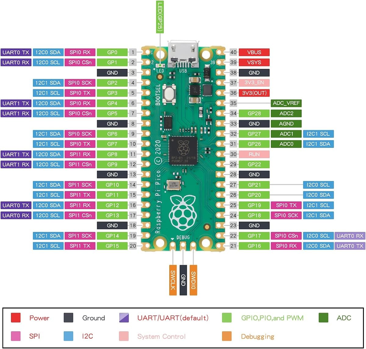
Answer in brief: The Raspberry Pi Pico has 26 GPIO pins, 3 ADC inputs, and PWM on every GPIO pin. It runs the RP2040 chip at a 133 megahertz clock and 3.3 volt logic. This guide maps each pin, the power pins, and the debug pins. It also covers the pins that are not general GPIO.

Quick Facts

Item Detail Source
Chip RP2040, dual-core Cortex-M0+ Raspberry Pi Pico Datasheet
Clock speed 133 megahertz Raspberry Pi Pico Datasheet
Logic voltage 3.3 volts, not 5 volt tolerant Raspberry Pi Pico Datasheet
Board edge 40 pins Raspberry Pi Pico Datasheet
GPIO pins 26 pins: GP0 to GP22 and GP26 to GP28 Raspberry Pi Pico Datasheet
ADC inputs 3 inputs: GP26, GP27, GP28, 12-bit RP2040 Datasheet
ADC range 0 counts to 4095 counts, 0 volts to 3.3 volts RP2040 Datasheet
Onboard LED GP25 Raspberry Pi Pico Datasheet
VSYS input range 1.8 volts to 5.5 volts Raspberry Pi Pico Datasheet
VBUS pin Pin 40, USB 5 volt input Raspberry Pi Pico Datasheet
3V3 output, max 300 milliamperes Raspberry Pi Pico Datasheet
PWM Every GPIO pin, 8 slices RP2040 Datasheet

Raspberry Pi Pico Pinout Table

This table is an original pinout table built from the Raspberry Pi Pico Datasheet. It is not a copied image. The GP names are the printed pin names on the board. The pin numbers are the board edge numbers.

Edge pin GP name Main function Notes
1 GP0 GPIO UART0 TX default
2 GP1 GPIO UART0 RX default
3 GND Ground Common ground
4 GP2 GPIO I2C1 SDA option
5 GP3 GPIO I2C1 SCL option
6 GP4 GPIO UART1 TX, I2C0 SDA default
7 GP5 GPIO UART1 RX, I2C0 SCL default
8 GND Ground Common ground
9 GP6 GPIO I2C1 SDA default
10 GP7 GPIO I2C1 SCL default
11 GP8 GPIO SPI1 RX default
12 GP9 GPIO SPI1 CSn default
13 GND Ground Common ground
14 GP10 GPIO SPI1 SCK default
15 GP11 GPIO SPI1 TX default
16 GP12 GPIO General use
17 GP13 GPIO General use
18 GND Ground Common ground
19 GP14 GPIO General use
20 GP15 GPIO General use
21 GP16 GPIO SPI0 RX default
22 GP17 GPIO SPI0 CSn default
23 GND Ground Common ground
24 GP18 GPIO SPI0 SCK default
25 GP19 GPIO SPI0 TX default
26 GP20 GPIO General use
27 GP21 GPIO General use
28 GND Ground Common ground
29 GP22 GPIO General use
30 RUN Reset Active low, pull low to reset
31 GP26 ADC0 Analog input, 12-bit
32 GP27 ADC1 Analog input, 12-bit
33 AGND Analog ground Ground for ADC use
34 GP28 ADC2 Analog input, 12-bit
35 ADC_VREF ADC reference 3.3 volt reference input
36 3V3(OUT) 3.3 volt output 300 milliamperes max
37 3V3_EN 3.3 volt enable Pull low to disable the regulator
38 GND Ground Common ground
39 VSYS Power input 1.8 volts to 5.5 volts input
40 VBUS Power input USB 5 volt input

Power Pins

Power the Pico through USB, the VBUS pin, or the VSYS pin. USB gives 5 volts to VBUS. VBUS is pin 40 on the board edge. VSYS is pin 39 on the board edge. VSYS accepts 1.8 volts to 5.5 volts. That range covers a battery pack and a 5 volt supply.

Use VSYS for battery power. A 3-cell pack or a single lithium cell with a boost stage can feed VSYS. Check the Pico Datasheet power section before you pick a battery. A battery above 5.5 volts can damage the board. A battery below 1.8 volts will not run the regulator.

The 3V3(OUT) pin is pin 36. It gives 3.3 volts at a max of 300 milliamperes. That value comes from the Raspberry Pi Pico Datasheet. Use it for sensors and small loads. A part that needs more current needs its own regulator.

Pin 37 is 3V3_EN. It enables the 3.3 volt regulator. Leave it alone for normal use. Pull it low only when you want to shut the regulator down. Pin 35 is ADC_VREF. It sets the ADC reference. Leave it at 3.3 volts for normal use.

Boot and Reset Pins

The Pico has a BOOTSEL button for firmware loading. Hold BOOTSEL while you plug in USB. The board then appears as a USB drive. Drag a UF2 file onto that drive to load new firmware. Release BOOTSEL after the drive appears. That path loads MicroPython, CircuitPython, or a C build.

Pin 30 is RUN. It resets the chip when pulled low. It is active low. Connect a button from RUN to ground for a manual reset. Release the button to let the chip run again. Do not hold RUN low for normal use.

ADC Pins

The Pico has 3 ADC inputs on the board edge: GP26, GP27, and GP28. They are ADC0, ADC1, and ADC2. Each input reads 12-bit values from 0 counts to 4095 counts. A 0 volt input reads 0 counts. A 3.3 volt input reads 4095 counts. That step size is about 0.8 millivolts per count at the default reference.

ADC3 is an internal channel. It reads VSYS through GP29. It does not appear on the board edge. Use ADC3 in code to check the supply voltage. That read helps a battery project track its own power.

PWM Pins

PWM works on every GPIO pin on the Pico. The RP2040 chip has 8 PWM slices. Each slice drives 2 pins. That gives 16 PWM channels across the 26 GPIO pins. The Pico Datasheet and the RP2040 Datasheet both list this layout.

PWM drives a signal, not a load. Use a transistor or a driver for a motor. Use a series resistor for an LED. RP2040 GPIO pins have four drive-strength settings, nominally 2, 4, 8, and 12 mA, per the RP2040 Datasheet, section 5.5.3.5. The highest setting is 12 mA per pin. The total current sourced by all GPIO and QSPI pins together must not exceed 50 mA, and the total sunk must not exceed 50 mA, per the same datasheet (IIOVDD_MAX and IIOVSS_MAX). Those are drive-strength modes, not hard per-pin limits, and the pin voltage sags as the load rises. Keep LED current low with a resistor.

I2C Pins

I2C0 uses GP4 for SDA and GP5 for SCL by default. I2C1 uses GP6 for SDA and GP7 for SCL by default. Those defaults are the common pin choices in Pico examples. The RP2040 chip can route I2C to many other pins. Check the RP2040 Datasheet pin function table before you move the bus.

I2C runs at 3.3 volt logic on this board. Check the device voltage before you connect it. A 5 volt I2C device needs a level shifter. A direct 5 volt connection can damage the Pico.

SPI Pins

SPI0 uses GP16 for RX, GP17 for CSn, GP18 for SCK, and GP19 for TX by default. SPI1 uses GP8 for RX, GP9 for CSn, GP10 for SCK, and GP11 for TX by default. Those defaults are the common pin choices in Pico examples. The RP2040 chip can route SPI to many other pins.

SPI runs at 3.3 volt logic on this board. Check the device voltage before you connect it. A 3.3 volt SPI device connects directly. A 5 volt SPI device needs a level shifter.

UART Pins

UART0 uses GP0 for TX and GP1 for RX by default. UART1 uses GP4 for TX and GP5 for RX by default. Those defaults are the common pin choices in Pico examples. The RP2040 chip can route UART to many other pins. Check the RP2040 Datasheet pin function table before you move the port.

The USB port carries a separate serial link for MicroPython and for debug output. That link does not use GP0 or GP1. You can use GP0 and GP1 for a device while the USB console stays open. That split is handy for GPS logging.

USB and SWD Debug Pins

For a Pico comparison, see the live post Raspberry Pi Pico vs Pico W vs Pico 2: Chip, Wireless, and Headers (live post #20577). For starter kit options, see the live post Raspberry Pi Pico Starter Kits Compared: SunFounder, LAFVIN, and More (live post #20579).

Pins to Avoid

Avoid GP23, GP24, GP25, and GP29 as general GPIO. They are internal pins. GP25 is the onboard LED on the Pico. Use it only for the LED. GP24 senses VBUS. GP29 monitors VSYS. GP23 controls power save.

On the Pico WH, GP23, GP24, GP25, and GP29 are used by the onboard wireless chip instead, per the Raspberry Pi Pico W Datasheet. The onboard LED on the Pico WH is driven by the wireless chip, not by GP25, so the GP25 LED blink in the sketch below works on the Pico only, not on the Pico WH. In MicroPython, use Pin(“LED”, Pin.OUT) on the Pico WH.

Avoid 5 volt logic on any GPIO pin. This board uses 3.3 volt logic only. It is not 5 volt tolerant. A 5 volt signal needs a level shifter. A direct 5 volt input can damage the pin.

Max Current and Logic Voltage

Logic voltage is 3.3 volts on every GPIO pin. That value comes from the Raspberry Pi Pico Datasheet. Treat 3.3 volts as the high level. Treat 0 volts as the low level. The board is not 5 volt tolerant. That warning is in the datasheet.

The 3V3(OUT) pin gives 3.3 volts at a max of 300 milliamperes. That value comes from the Raspberry Pi Pico Datasheet. Treat 300 milliamperes as the working limit for that pin. A larger load needs its own regulator.

The RP2040 GPIO pins have four drive-strength settings, nominally 2, 4, 8, and 12 mA, per the RP2040 Datasheet, section 5.5.3.5. The highest setting is 12 mA per pin. The total current sourced by all GPIO and QSPI pins together must not exceed 50 mA, and the total sunk must not exceed 50 mA (IIOVDD_MAX and IIOVSS_MAX). Treat 12 mA per pin and 50 mA total as the working limits.

Use a driver for any load above a small LED. Keep LED current low with a series resistor. A 220 ohm resistor is a common bench value for a 3.3 volt LED test. Check the LED datasheet for its own forward voltage before you pick a resistor.

Wiring and Power Warnings

Power the board before you connect a sensor. Keep the USB cable short. Use a cable under 3 feet for bench tests when you can. Long wires pick up noise. Noise causes ADC jitter and I2C errors.

Do not feed 5 volts into a GPIO pin. Do not feed 5 volts into the 3V3(OUT) pin. Do not feed more than 5.5 volts into VSYS. Each of those mistakes can damage the board. Check the pin labels before every connection.

Pin Test Sketch

Language: MicroPython. Firmware: MicroPython version 1.22.2 for RP2040. No extra library install is needed for this test. Load the firmware with the BOOTSEL drive method. Code status: code not compiled. No arduino-cli or PlatformIO is installed in this environment.

# Raspberry Pi Pico pin test script
# Language: MicroPython version 1.22.2 for RP2040
# Board: Raspberry Pi Pico, RP2040
# Code status: code not compiled

from machine import Pin, ADC, PWM
import time

# Onboard LED is GP25 on the Pico. On the Pico WH the LED is on the wireless chip, not GP25.
led = Pin(25, Pin.OUT)

# ADC test uses GP26, which is ADC0.
adc = ADC(Pin(26))

# PWM test uses GP15 at 1000 hertz.
pwm = PWM(Pin(15))
pwm.freq(1000)  # Set PWM frequency to 1000 hertz.
pwm.duty_u16(0)  # Start with the output off.

# UART test uses UART0 on GP0 TX and GP1 RX.
# The USB console stays free for print output.
from machine import UART
uart = UART(0, baudrate=9600, tx=Pin(0), rx=Pin(1))

print("Pico pin test started")

while True:
    # Read the ADC value on GP26.
    # ADC range is 0 to 65535 counts in MicroPython.
    value = adc.read_u16()
    print("GP26 ADC value:", value)

    # Convert the ADC value to a voltage from 0 to 3.3 volts.
    volts = value * 3.3 / 65535
    print("GP26 volts:", volts)

    # Fade the PWM output on GP15 from off to full.
    for level in range(0, 65536, 4096):
        pwm.duty_u16(level)
        time.sleep(0.05)  # Wait 50 milliseconds per step.

    # Blink the onboard LED on GP25 once per loop.
    led.on()
    time.sleep(0.5)  # Wait 500 milliseconds.
    led.off()
    time.sleep(0.5)  # Wait 500 milliseconds.

Expected result: the console shows a GP26 ADC value and a voltage each loop. The value changes with the voltage on GP26. The PWM output on GP15 fades up in steps. The onboard LED blinks once per loop. If no console output appears, check the MicroPython firmware load and the serial port selection.

Frequently Asked Questions

How many GPIO pins does the Pico have?

It has 26 GPIO pins: GP0 through GP22, plus GP26, GP27, and GP28. GP23, GP24, GP25, and GP29 are internal pins. They do not appear on the board edge as general GPIO.

Which pins are ADC on the Pico?

GP26 is ADC0, GP27 is ADC1, and GP28 is ADC2. Each input reads 12-bit values from 0 counts to 4095 counts. ADC3 is an internal channel that reads VSYS.

Is the Pico 5 volt tolerant?

No, the Pico is not 5 volt tolerant. It uses 3.3 volt logic only. A 5 volt signal needs a level shifter. A direct 5 volt input can damage the pin.

How do I load MicroPython on the Pico?

Hold BOOTSEL while you plug in USB. The board appears as a USB drive. Drag the MicroPython UF2 file onto that drive. The board reboots with MicroPython running.

Boards That Match This Pinout

These boards use the pinout in this guide. Check the product page for current stock before you order. Stock changes over time.

Related reading: compare this board with ESP32 boards in the staged pillar RP2040 vs ESP32 (row 24, staged). For sibling pinouts, see Arduino UNO R3 Pinout and Nano V3.0 USB-C Guide: ATmega328P Board for Arduino IDE.

Sources

  • Raspberry Pi Pico Datasheet, https://datasheets.raspberrypi.com/pico/pico-datasheet.pdf
  • RP2040 Datasheet, https://datasheets.raspberrypi.com/rp2040/rp2040-datasheet.pdf
  • Raspberry Pi Pico W Datasheet, https://pip.raspberrypi.com/documents/RP-008312-DS-pico-w-datasheet.pdf
  • Raspberry Pi Pico pinout guide, https://www.raspberrypi.com/documentation/microcontrollers/raspberry-pi-pico.html

Last updated 2026-11-21.

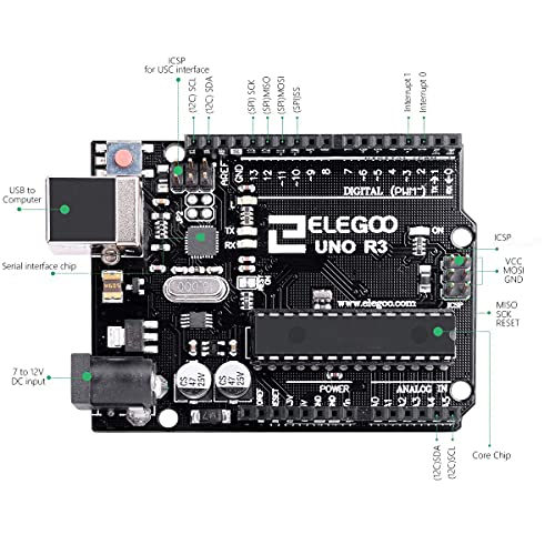
Arduino UNO R3 Pinout: Digital, Analog, PWM, and Power

Push button wired to an Arduino input pin with a 10k pull-up resistor

Arduino UNO R3 Pinout: Digital, Analog, PWM, and Power

Answer in brief: The Arduino UNO R3 has 14 digital pins, 6 analog inputs, and 6 PWM pins. It runs on 5 volt logic at a 16 megahertz clock. This guide maps each pin, the power pins, and the current limits. It also covers I2C, SPI, UART, and the pins to avoid.

Quick Facts

Item Detail Source
Chip ATmega328P Arduino UNO R3 documentation
Clock speed 16 megahertz Arduino UNO R3 documentation
Logic voltage 5 volts Arduino UNO R3 documentation
Digital pins 14 pins, D0 to D13 Arduino UNO R3 documentation
PWM pins 6 pins: D3, D5, D6, D9, D10, D11 Arduino UNO R3 documentation
Analog inputs 6 inputs, A0 to A5, 10-bit Microchip ATmega328P datasheet DS40002061B
Analog range 0 counts to 1023 counts Microchip ATmega328P datasheet DS40002061B
Per-pin current, recommended 20 milliamperes Microchip ATmega328P datasheet DS40002061B
Per-pin current, absolute max 40 milliamperes Microchip ATmega328P datasheet DS40002061B
Chip total current 200 milliamperes Microchip ATmega328P datasheet DS40002061B
3V3 output, max About 50 milliamperes Arduino UNO R3 documentation
VIN range, recommended 7 volts to 12 volts Arduino UNO R3 documentation

Arduino UNO R3 Pinout Table

This table is an original pinout table built from the Arduino UNO R3 documentation. It is not a copied image. The D names are the printed header names on the board. Use the table with the board in front of you.

Pin Function Shared functions
D0 Digital I/O UART RX
D1 Digital I/O UART TX
D2 Digital I/O Interrupt INT0
D3 Digital I/O, PWM Interrupt INT1, PWM at 490 hertz
D4 Digital I/O None
D5 Digital I/O, PWM PWM at 980 hertz
D6 Digital I/O, PWM PWM at 980 hertz
D7 Digital I/O None
D8 Digital I/O None
D9 Digital I/O, PWM PWM at 490 hertz
D10 Digital I/O, PWM SPI SS, PWM at 490 hertz
D11 Digital I/O, PWM SPI MOSI, PWM at 490 hertz
D12 Digital I/O SPI MISO
D13 Digital I/O SPI SCK, onboard LED
A0 Analog input Digital pin D14
A1 Analog input Digital pin D15
A2 Analog input Digital pin D16
A3 Analog input Digital pin D17
A4 Analog input Digital pin D18, I2C SDA
A5 Analog input Digital pin D19, I2C SCL
VIN Power input 7 volts to 12 volts recommended
5V Power output 5 volt rail from USB or regulator
3V3 Power output 3.3 volt output, about 50 milliamperes max
GND Ground Common ground for all wiring
IOREF Reference Board logic voltage, 5 volts
AREF Reference Analog reference input
RESET Reset Pull low to restart the chip

Power Pins

Power the UNO R3 through USB, the barrel jack, or the VIN pin. The barrel jack and VIN accept 7 volts to 12 volts. The on-board regulator drops that input to 5 volts. A higher input makes the regulator run hotter. Keep the input near 9 volts for bench work when you can.

The 5V pin is a 5 volt output when USB or the jack powers the board. It can also act as a 5 volt input. Feed it only with a clean, regulated 5 volt supply. Do not feed it with a higher voltage. The 3V3 pin gives 3.3 volts at about 50 milliamperes max. Use it only for small 3.3 volt parts.

IOREF tells a shield the board logic voltage. On this board, IOREF is 5 volts. AREF sets the top of the analog range. Leave AREF unconnected for normal use. The default reference is 5 volts. Ground pins appear on both headers. Use the nearest ground for each part.

Boot and Reset Pins

The UNO R3 has no strapping pins like an ESP32 board. It starts code on power-up or reset. The RESET pin restarts the chip when pulled low. The on-board RESET button does the same job. A shield can also pull RESET low.

Uploads use the USB port and the on-board USB-to-serial chip. The IDE resets the board through the serial link. No jumper is needed for normal uploads. If an upload fails, press RESET once and try again. Check the board and port selection in the IDE first.

The ICSP header near the chip carries SPI and reset for direct programming. Most users never need it. Leave it alone unless you program the chip with an external programmer. A wrong ICSP connection can erase the bootloader.

ADC Pins

The UNO R3 has 6 analog inputs, A0 through A5. Each input reads 10-bit values from 0 counts to 1023 counts. A 0 volt input reads 0 counts. A 5 volt input reads 1023 counts. That step size is about 4.9 millivolts per count at the default reference.

A0 through A5 also work as digital pins D14 through D19. Use them as digital outputs when you run out of digital pins. Set the pin mode in code. A pin cannot read analog and drive digital at the same time.

PWM Pins

PWM is available on 6 pins: D3, D5, D6, D9, D10, and D11. The PWM frequency is 490 hertz on D3, D9, D10, and D11. It is 980 hertz on D5 and D6. That split matters for some loads. A motor driver may buzz at one frequency and run smooth at the other.

PWM drives a signal, not a load. Use a transistor or a driver for a motor. Use a series resistor for an LED. A PWM pin still follows the 20 milliampere recommended limit. Do not connect a motor directly to a PWM pin.

I2C Pins

I2C uses A4 for SDA and A5 for SCL. Those two analog pins carry the bus. Connect a display or a sensor to those two pins. Share the bus with more than one device when each device has a different address.

A4 and A5 cannot read analog while they run the I2C bus. Plan the pin budget when you need both I2C and analog reads. Use A0 through A3 for analog in that case. That leaves A4 and A5 free for the bus.

SPI Pins

SPI uses D10 for SS, D11 for MOSI, D12 for MISO, and D13 for SCK. Those four pins carry the bus. Pick a different digital pin for a second chip select when you add a second SPI device. D10 must stay an output for the board to act as SPI master.

SPI runs at 5 volt logic on this board. Check the device voltage before you connect it. A 3.3 volt SPI device needs a level shifter. A direct 5 volt connection can damage a 3.3 volt part.

UART Pins

UART uses D0 for RX and D1 for TX. Those pins connect to the USB-to-serial chip. They carry the serial monitor link. They also carry uploads. Do not connect a GPS module to D0 and D1 while you debug over USB. The two uses clash.

Keep the baud rate the same on both ends of a UART link. A mismatch gives garbled text. Start at 9600 baud for a new device. Raise the rate only after the link works.

USB Pins

The UNO R3 has a USB port for power and programming. The product in this guide uses a USB cable in the box. Check the product page for the cable type in your pack. The USB link powers the board at 5 volts. It also carries uploads and serial debug output.

The USB port does not expose D0 and D1 as separate pads. Those pins are the UART lines behind the USB chip. Treat D0 and D1 as busy during uploads. Free them only after the upload ends.

Pins to Avoid

Avoid D0 and D1 for sensors while you debug over USB. Avoid A4 and A5 for analog reads while I2C is active. Avoid D10 as a general input when SPI runs as master. It must stay an output in that mode.

Avoid AREF as a power output. It is a reference input only. Avoid feeding 5 volts into the 3V3 pin. Avoid feeding more than 5 volts into the 5V pin. Both mistakes can damage the regulator or the chip.

Avoid a load above 20 milliamperes on any single pin. Avoid a total load above 200 milliamperes across the chip. Those limits come from the Microchip ATmega328P datasheet DS40002061B. Stay under them for a long board life.

Max Current and Logic Voltage

Logic voltage is 5 volts on every digital pin. That value comes from the Arduino UNO R3 documentation. Treat 5 volts as the high level. Treat 0 volts as the low level. A 3.3 volt sensor output may read as high on a 5 volt input, but check the sensor datasheet first.

The recommended current per pin is 20 milliamperes. The absolute max per pin is 40 milliamperes. The chip total is 200 milliamperes. Those three numbers come from the Microchip ATmega328P datasheet DS40002061B. Treat 20 milliamperes as the working limit. Treat 40 milliamperes as a damage threshold, not a target.

The 3V3 output gives about 50 milliamperes max. That value comes from the Arduino UNO R3 documentation. Use it only for small 3.3 volt parts. A WiFi module or a large display needs its own regulator.

Wiring and Power Warnings

Power the board before you connect a sensor. Keep the USB cable short. Use a cable under 3 feet for bench tests when you can. Long wires pick up noise. Noise causes analog jitter and I2C errors.

Use a series resistor for every LED. A 220 ohm resistor is a common bench value for a 5 volt LED test. Check the LED datasheet for its own forward voltage before you pick a resistor. A LED with no resistor can draw too much current from the pin.

Use a driver for any motor, relay, or solenoid. The GPIO pin only signals the driver. The driver handles the load current. A direct motor connection can damage the pin and reset the board.

Pin Test Sketch

Language: Arduino. Library: Arduino AVR core version 1.8.6, with no extra library install. Code status: code not compiled. No arduino-cli or PlatformIO is installed in this environment.

// Arduino UNO R3 pin test sketch
// Board: UNO R3, ATmega328P
// Arduino AVR core version 1.8.6
// Code status: code not compiled

// PWM test pin is D9. It runs at 490 hertz.
const int pwmPin = 9;
// Analog test pin is A0. It reads 0 to 1023 counts.
const int analogPin = A0;
// Onboard LED pin is D13.
const int ledPin = 13;

void setup() {
  // Start serial at 9600 baud for debug output.
  Serial.begin(9600);
  delay(500); // Wait 500 milliseconds for the monitor.

  // Set the PWM pin and the LED pin as outputs.
  pinMode(pwmPin, OUTPUT);
  pinMode(ledPin, OUTPUT);

  Serial.println("UNO R3 pin test started");
}

void loop() {
  // Read the analog value on A0.
  int adcValue = analogRead(analogPin);
  Serial.print("A0 value: ");
  Serial.println(adcValue);

  // Fade the PWM output on D9 from off to full.
  for (int level = 0; level <= 255; level += 5) {
    analogWrite(pwmPin, level);
    delay(20); // Wait 20 milliseconds per step.
  }

  // Blink the onboard LED on D13 once per loop.
  digitalWrite(ledPin, HIGH);
  delay(500); // Wait 500 milliseconds.
  digitalWrite(ledPin, LOW);
  delay(500); // Wait 500 milliseconds.
}

Expected result: the serial monitor shows an A0 value each loop. The value changes with the voltage on A0. The PWM output on D9 fades up in steps. The onboard LED blinks once per loop. If no serial output appears, check the board and port selection in the IDE.

Frequently Asked Questions

How many digital pins does the UNO R3 have?

It has 14 digital pins, D0 through D13. Six of those pins support PWM. The analog pins A0 through A5 can also work as digital pins D14 through D19.

Which pins are PWM on the UNO R3?

PWM pins are D3, D5, D6, D9, D10, and D11. D5 and D6 run at 980 hertz. The other four PWM pins run at 490 hertz.

What is the current limit per pin?

The recommended limit is 20 milliamperes per pin. The absolute max is 40 milliamperes per pin. The chip total is 200 milliamperes. Stay under the recommended limit for normal use.

Can I power the UNO R3 from the VIN pin?

Yes, feed VIN with 7 volts to 12 volts. The on-board regulator drops that input to 5 volts. Keep the input near 9 volts for bench work. A higher input makes the regulator run hotter.

Boards That Match This Pinout

These boards use the pinout in this guide. Check the product page for current stock before you order. Stock changes over time.

Related reading: compare this board with other microcontroller families in the staged pillar RP2040 vs ESP32 (row 24, staged). For a first project, see the live post How to Start with a UNO R3 Board for Arduino Projects (live post #15177) and the live post How to Build Your First Arduino Project with UNO and OLED (live post #15203). For sibling pinouts, see Nano V3.0 USB-C Guide: ATmega328P Board for Arduino IDE and Raspberry Pi Pico Pinout.

Sources

  • Arduino UNO R3 documentation, https://docs.arduino.cc/hardware/uno-rev3/
  • Microchip ATmega328P datasheet DS40002061B, https://ww1.microchip.com/downloads/en/DeviceDoc/Atmel-7810-Automotive-Microcontrollers-ATmega328P_Datasheet.pdf
  • Arduino UNO R3 schematic, https://docs.arduino.cc/hardware/uno-rev3/

Last updated 2026-11-21.

Seeed XIAO ESP32S3 Pinout: GPIO, Camera, and Power

XIAO ESP32S3 board with USB-C port and pin pads. Caption: XIAO ESP32S3 board with USB-C port. Description: Top view of the XIAO ESP32S3 board used in this pinout guide.

XIAO ESP32S3 Pinout: GPIO, Camera, and Power Pins

Answer in brief: The XIAO ESP32S3 gives you 11 GPIO pins, named D0 through D10. It also gives you native USB, I2C, SPI, UART, and ADC on those same pins. The Sense version adds a camera and a microSD card on a rear connector. This guide maps each pin and its shared uses.

Quick Facts

Item Detail Source
Board XIAO ESP32S3 Seeed Studio XIAO ESP32S3 wiki
GPIO pins 11 pins, D0 to D10 Seeed Studio XIAO ESP32S3 wiki
Logic voltage 3.3 volts Seeed Studio XIAO ESP32S3 wiki
USB port USB-C, native USB Seeed Studio XIAO ESP32S3 wiki
Native USB pins GPIO19 D- and GPIO20 D+ Seeed Studio XIAO ESP32S3 wiki
Boot pin GPIO0 Seeed Studio XIAO ESP32S3 wiki
I2C pins D4 SDA and D5 SCL Seeed Studio XIAO ESP32S3 wiki
SPI pins D8 SCK, D9 MISO, D10 MOSI Seeed Studio XIAO ESP32S3 wiki
UART pins D6 TX and D7 RX Seeed Studio XIAO ESP32S3 wiki
Sense SD chip select GPIO21 Seeed Studio XIAO ESP32S3 wiki

XIAO ESP32S3 Pinout Table

This table is an original pinout table built from the Seeed wiki pin multiplexing page. It is not a copied image. The D names are the printed pad names on the board. The GPIO numbers are the chip pin numbers in code.

Pad GPIO Main function Shared functions
D0 GPIO1 ADC input Touch input
D1 GPIO2 ADC input Touch input
D2 GPIO3 ADC input Touch input, strapping pin
D3 GPIO4 ADC input Touch input
D4 GPIO5 I2C SDA ADC input, touch input
D5 GPIO6 I2C SCL ADC input, touch input
D6 GPIO43 UART TX UART transmit only
D7 GPIO44 UART RX UART receive only
D8 GPIO7 SPI SCK ADC input, touch input
D9 GPIO8 SPI MISO ADC input, touch input
D10 GPIO9 SPI MOSI ADC input, touch input
BOOT GPIO0 Boot button Hold low at reset for download mode
5V Power 5 volt input USB 5 volt rail when USB is connected
3V3 Power 3.3 volt output Power for low-current 3.3 volt parts
GND Power Ground Common ground for all wiring

Power Pins

Power the board through the USB-C port or the 5V pad. The USB-C port supplies 5 volts from the host. The 5V pad accepts 5 volts from an external supply. Use one 5 volt source at a time. Do not feed 5 volts into the 3V3 pad.

The 3V3 pad is a 3.3 volt output from the SGM6029 buck converter on the board. The schematic v1.3 marks that converter Imax 600 mA, so keep external 3.3 volt loads under 600 mA in total. The Seeed wiki says 700 mA can be drawn from the 3V3 pad, which is above the schematic Imax, so the 600 mA schematic figure is the safe limit to plan on. The 5V pad is the USB VBUS rail. No separate 5V input current limit is published in schematic v1.3, so the USB source and cable set that limit in practice.

Strapping and Boot Pins

GPIO0 is the BOOT pin. The board has a BOOT button tied to GPIO0. Hold BOOT low at reset to enter download mode. The Arduino IDE and esptool handle this step in most cases. Press BOOT only when an upload fails to start.

GPIO3 on pad D2 is also a strapping pin. Keep D2 free of strong pull-downs at boot. A wrong level at boot can change the boot mode. Check the Seeed wiki strapping notes before you wire a sensor to D2.

ADC and Touch Pins

ADC input is available on D0, D1, D2, D3, D4, D5, D8, D9, and D10. That is 9 ADC pins in total. Each ADC pin reads a voltage from 0 volts to 3.3 volts. Use a voltage divider for any higher voltage. Never feed 5 volts into an ADC pin.

D11 is GPIO42 and D12 is GPIO41 on Sense and Plus variants. Those two pins serve the PDM microphone on the Sense board. Note that D11 and D12 do not support ADC on the S3 chip. Do not plan an analog read on those two pins. Use them only for their Sense roles unless the wiki for your variant says otherwise.

PWM Pins

PWM output works on the GPIO pins through the LEDC peripheral. Use PWM for a dim LED, a small buzzer, or a servo signal. The servo signal is a control signal only. It does not power the servo. Power the servo from a separate supply.

Every D pad can carry a PWM signal in code. The limit is the pin count, not the PWM peripheral. Pick a free D pad for each PWM output. Keep I2C and SPI pins free when those buses are in use. A PWM output on D4 would clash with I2C SDA.

I2C Pins

I2C uses D4 for SDA and D5 for SCL. The chip GPIO numbers are GPIO5 and GPIO6. Those two pins are the default I2C pair in most XIAO examples. Use them for an OLED display, a sensor, or a real-time clock.

Both I2C pins also support ADC and touch. That sharing means a choice. A pin on the I2C bus cannot read an analog voltage at the same time. Plan the pin budget before you add a second sensor.

SPI Pins

SPI uses D8 for SCK, D9 for MISO, and D10 for MOSI. The chip GPIO numbers are GPIO7, GPIO8, and GPIO9. Pick any free GPIO pin for the SPI chip select. D0 is a common chip select choice when it is free.

All three SPI pins also support ADC and touch. That sharing is the same trade as I2C. A SPI device claims all three pins. Plan for that claim before you add an analog sensor to D8, D9, or D10.

UART Pins

UART uses D6 for TX and D7 for RX. The chip GPIO numbers are GPIO43 and GPIO44. Those two pins carry the hardware serial port on the board pads. Use them for a GPS module, a serial sensor, or a second microcontroller.

The USB-C port carries a separate native USB serial link. That link is the programming and debug console. It does not use D6 or D7. You can use D6 and D7 for a device while the USB console stays open. That split is handy for GPS logging.

USB Pins

Native USB uses GPIO19 for D- and GPIO20 for D+. Those pins are internal. They do not appear on the D pads. The USB-C connector ties to them on the board. You cannot reassign them to other uses.

Native USB supports serial, HID, and mass storage modes in code. The Arduino core exposes USB serial by default. Use the USB link for uploads and debug output. Use D6 and D7 when you need a separate hardware UART.

Sense Camera and SD Card

The Sense version adds an OV2640 camera and a microSD card slot. Both sit on a rear board-to-board connector. The standard XIAO ESP32S3 has no camera and no SD slot. Check which version you hold before you follow the Sense wiring.

Sense feature Detail Source
Camera OV2640 on rear connector Seeed Studio XIAO ESP32S3 wiki
SD card chip select GPIO21 Seeed Studio XIAO ESP32S3 wiki
PDM microphone pins GPIO42 and GPIO41 Seeed Studio XIAO ESP32S3 wiki
Standard board camera None fitted Seeed Studio XIAO ESP32S3 wiki

The Sense camera uses the rear connector, not the D pads. That design keeps D0 through D10 free for your own wiring, except for the SD card sharing below. The SD card chip select is GPIO21. The SD card shares the SPI lines D8, D9, and D10, which are GPIO7, GPIO8, and GPIO9, with chip select on GPIO21. Do not put a second SPI device on D8, D9, and D10 while the SD card is mounted unless it has its own chip select pin. GPIO21 is also the user LED, so the LED flickers with card access.

For the Sense board guide, see the live post Seeed XIAO ESP32S3 Guide: Standard Board vs Sense Board (live post #18362). That guide compares the standard board and the Sense board in full.

Pins to Avoid

Avoid GPIO19 and GPIO20 for general wiring. They are the native USB pins. Avoid GPIO0 as a permanent output. It is the BOOT pin. Avoid D2 as a boot-time output. It is a strapping pin.

Avoid D11 and D12 for ADC reads. Those pins do not support ADC on the S3 chip. Avoid 5 volt logic on any D pad. This board uses 3.3 volt logic. A 5 volt signal needs a level shifter.

Avoid using D4 and D5 for other roles when I2C is active. Avoid D8, D9, and D10 for other roles when SPI is active. A shared pin causes a clash that is hard to trace in code.

Max Current and Logic Voltage

Logic voltage is 3.3 volts on every D pad. That value comes from the Seeed Studio XIAO ESP32S3 wiki. Treat 3.3 volts as the high level. Treat 0 volts as the low level. Keep sensor outputs at 3.3 volts or below.

At the strongest drive setting, a GPIO pin sources about 40 mA (IOH) and sinks about 28 mA (IOL), per the Espressif ESP32-S3 Series Datasheet v2.2, Table 5-4. Those are drive-strength values at 3.3 volts, not a recommended continuous load. Cumulative IO output current for the chip is 1500 mA at absolute maximum, per section 5.1 of the same datasheet. Treat a small LED through a resistor as the practical per-pin load, not 40 mA.

Use a driver for any load above a small LED. Keep LED current low with a series resistor. A 220 ohm resistor is a common bench value for a 3.3 volt LED test. Check the LED datasheet for its own forward voltage before you pick a resistor.

Wiring and Power Warnings

Power the board at 5 volts through USB-C or the 5V pad. Do not feed 5 volts into the 3V3 pad. Double-check the pad labels before you connect power. The pads are small and close together.

Keep wires short. Use a cable under 3 feet for bench tests when you can. Long wires pick up noise. Noise causes I2C errors and ADC jitter. Twist power and ground wires together when the run is long.

Solder the header pins with care. A solder bridge between two small pads shorts the board. Check each joint with a magnifier. Test for shorts with a meter before first power-up. A short on the 5 volt rail can damage the USB host.

Pin Test Sketch

Language: Arduino. Library: Arduino ESP32 core version 2.0.14. No extra library install is needed for this test. Code status: code not compiled. No arduino-cli or PlatformIO is installed in this environment.

// XIAO ESP32S3 pin test sketch
// Board: XIAO ESP32S3
// Arduino ESP32 core version 2.0.14
// Code status: code not compiled

// D pad to GPIO map from the Seeed wiki.
const int pinD0 = 1;  // ADC and touch.
const int pinD1 = 2;  // ADC and touch.
const int pinD4 = 5;  // I2C SDA, ADC, touch.
const int pinD5 = 6;  // I2C SCL, ADC, touch.
const int pinD6 = 43; // UART TX.
const int pinD7 = 44; // UART RX.
const int pinD8 = 7;  // SPI SCK, ADC, touch.

void setup() {
  // Start USB serial at 115200 baud for debug output.
  Serial.begin(115200);
  delay(1000); // Wait 1 second for the monitor to open.

  // Set D0 as an output for the blink test.
  pinMode(pinD0, OUTPUT);

  // Set the ADC pins as inputs.
  pinMode(pinD1, INPUT);
  pinMode(pinD4, INPUT);
  pinMode(pinD5, INPUT);

  Serial.println("XIAO ESP32S3 pin test started");
}

void loop() {
  // Read the ADC value on D1.
  // ADC range is 0 to 4095 counts on the ESP32-S3.
  int adcValue = analogRead(pinD1);
  Serial.print("D1 ADC value: ");
  Serial.println(adcValue);

  // Blink D0 for 500 milliseconds on and 500 milliseconds off.
  digitalWrite(pinD0, HIGH);
  delay(500); // Wait 500 milliseconds.
  digitalWrite(pinD0, LOW);
  delay(500); // Wait 500 milliseconds.
}

Expected result: the serial monitor shows a D1 ADC value each 1 second. The value changes when you touch a wire on D1 or feed it a voltage below 3.3 volts. The D0 output blinks at a 1 second period. If no serial output appears, check the USB cable and the board selection in the IDE.

Frequently Asked Questions

How many GPIO pins does the XIAO ESP32S3 have?

It has 11 GPIO pins on the pads, named D0 through D10. The GPIO numbers run from GPIO1 to GPIO9, plus GPIO43 and GPIO44. Native USB uses GPIO19 and GPIO20 internally.

Which pins are I2C on the XIAO ESP32S3?

D4 is SDA and D5 is SCL. The chip numbers are GPIO5 and GPIO6. Both pins also support ADC and touch. They cannot serve two roles at once.

Does the standard XIAO ESP32S3 have a camera?

No, the standard board has no camera. The Sense version adds an OV2640 camera and a microSD slot on a rear connector. The SD chip select is GPIO21 on the Sense board.

Can I use 5 volt sensors with this board?

No, not directly. The board uses 3.3 volt logic. A 5 volt sensor output needs a level shifter. A direct 5 volt input can damage the pin.

Boards That Match This Pinout

These boards use the pinout in this guide. Check the product page for current stock before you order. Stock changes over time.

Related reading: compare this board with the wider ESP32 family in the staged pillar ESP32 vs ESP32-S3 vs ESP32-C3 vs ESP32-C6 (row 22, staged). For sibling pinouts, see ESP32-CAM Pinout and ESP32 38-Pin Boards Compared: Narrow, DevKitC, and 32E.

Sources

  • Seeed Studio XIAO ESP32S3 pin multiplexing, https://wiki.seeedstudio.com/xiao_esp32s3_pin_multiplexing/
  • Seeed Studio XIAO ESP32S3 wiki, https://wiki.seeedstudio.com/xiao_esp32s3_getting_started/
  • Seeed Studio XIAO ESP32S3 schematic version 1.3, https://wiki.seeedstudio.com/xiao_esp32s3_getting_started/
  • Espressif ESP32-S3 Datasheet v2.2, https://www.espressif.com/sites/default/files/documentation/esp32-s3_datasheet_en.pdf

Last updated 2026-11-21.

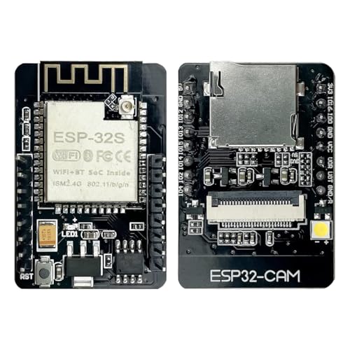
ESP32-CAM Pinout: Camera, SD Card, and Free GPIO Pins

ESP32-CAM board with OV2640 camera module and pin headers. Caption: ESP32-CAM board with OV2640 camera module. Description: Front view of the ESP32-CAM board used in this pinout guide.

ESP32-CAM Pinout: Camera, SD Card, and Free GPIO Pins

Answer in brief: The ESP32-CAM uses most of its GPIO pins for the camera and the microSD card. Only a small set of pins stays free for sensors and outputs. This guide maps the camera pins, the SD card pins, and the free pins. It also covers power, boot mode, and safe wiring.

Quick Facts

Item Detail Source
Board AI-Thinker ESP32-CAM Espressif ESP32 Series Datasheet
Logic voltage 3.3 volts Espressif ESP32 Series Datasheet
USB port None on board ESP32-CAM camera driver pin map
Programming pins GPIO1 TX and GPIO3 RX ESP32-CAM camera driver pin map
Flash mode pin GPIO0 held low at reset ESP32-CAM camera driver pin map
Camera pins used 15 pins ESP32-CAM camera driver pin map
SD card pins in 4-bit mode 6 pins ESP32-CAM camera driver pin map
SD card pins in 1-bit mode 3 pins ESP32-CAM camera driver pin map
Free pins with no SD card 6 pins ESP32-CAM camera driver pin map

ESP32-CAM Pinout Table

This table is an original pinout table built from the source data listed below. It is not a copied image. Check the board print against this table before you wire anything. Some boards print VCC on one header and 5V on the other header.

Header pin label GPIO Function Notes
5V Power 5 volt input Use a stable 5 volt supply
GND Power Ground Common ground for all wiring
GPIO12 GPIO12 SD DATA2, ADC, touch Free only when SD card is not used
GPIO13 GPIO13 SD DATA3, ADC, touch Free only when SD card is not used
GPIO15 GPIO15 SD CMD, ADC, touch, strapping Free only when SD card is not used
GPIO14 GPIO14 SD CLK, ADC, touch Free only when SD card is not used
GPIO2 GPIO2 SD DATA0, ADC, touch, strapping Free only when SD card is not used
GPIO4 GPIO4 SD DATA1, ADC, touch Free only when SD card is not used
3V3 Power 3.3 volt output Do not use as a 5 volt input
GPIO16 GPIO16 PSRAM chip select Do not use for other wiring
GPIO0 GPIO0 Camera XCLK, strapping, boot Hold low at reset for flash mode
GND Power Ground Common ground for all wiring
VCC Power 5 volt input Same 5 volt rail as the 5V pin
U0R GPIO3 UART receive Connect to adapter TX for programming
U0T GPIO1 UART transmit Connect to adapter RX for programming
GND Power Ground Common ground for all wiring

Power Pins

The board takes 5 volts through the 5V pin or the VCC pin. Both pins sit on the same 5 volt rail on this board. Use one 5 volt input at a time. Do not feed 5 volts into the 3V3 pin. That mistake can damage the board.

Strapping and Boot Pins

GPIO0 controls flash mode. Hold GPIO0 low at reset to enter flash mode. Release it after programming starts. Normal run mode needs GPIO0 high or floating at reset. A jumper wire to ground works for this step. Remove the jumper after the upload.

GPIO0 also carries the camera clock, XCLK. That dual role is normal on this board. Do not add a permanent pull-down to GPIO0. A permanent pull-down would force flash mode at every reset. Use a temporary jumper only during programming.

GPIO2 and GPIO15 are also strapping pins. They share SD card duties on this board. Keep them free of strong pull-downs at boot when the SD card is in use. Check the Espressif ESP32 Series Datasheet for the full strapping table before you add boot-time wiring.

Camera Pins

The camera uses 15 pins on this board. Those pins are fixed. Do not reassign them to other parts. The list below is the camera driver pin map for the AI-Thinker board.

Camera signal GPIO Notes
Data D0 GPIO5 Camera data line
Data D1 GPIO18 Camera data line
Data D2 GPIO19 Camera data line
Data D3 GPIO21 Camera data line
Data D4 GPIO36 Camera data line, input only
Data D5 GPIO39 Camera data line, input only
Data D6 GPIO34 Camera data line, input only
Data D7 GPIO35 Camera data line, input only
XCLK GPIO0 Camera clock, also boot pin
PCLK GPIO22 Camera pixel clock
VSYNC GPIO25 Camera vertical sync
HREF GPIO23 Camera horizontal reference
SDA GPIO26 Camera control bus data
SCL GPIO27 Camera control bus clock
PWDN GPIO32 Camera power down control

SD Card Pins

The microSD slot uses 6 pins in 4-bit mode. That mode gives the fastest SD writes on this board. The 6 pins are GPIO14, GPIO15, GPIO2, GPIO4, GPIO12, and GPIO13. All 6 pins are then busy. No free GPIO remains from that set while 4-bit mode runs.

SD signal GPIO Mode
CLK GPIO14 4-bit and 1-bit
CMD GPIO15 4-bit and 1-bit
DATA0 GPIO2 4-bit and 1-bit
DATA1 GPIO4 4-bit only
DATA2 GPIO12 4-bit only
DATA3 GPIO13 4-bit only

Free GPIO Pins

Free pins depend on SD card use. With no SD card, 6 pins are free. Those pins are GPIO2, GPIO4, GPIO12, GPIO13, GPIO14, and GPIO15. With 1-bit SD mode, 3 pins are free. Those pins are GPIO4, GPIO12, and GPIO13. With 4-bit SD mode, none of those 6 pins are free.

GPIO33 is the red LED pin. You can blink it in code. It is not a good general output for a load. GPIO16 is the PSRAM chip select. Leave GPIO16 alone. GPIO32 is the camera power-down pin. Leave it under camera driver control.

ADC, Touch, and PWM

GPIO2, GPIO4, GPIO12, GPIO13, GPIO14, and GPIO15 all support ADC input. They also support touch input on the ESP32 chip. That overlap is useful. It is also a limit. A pin in SD use cannot serve as an ADC input at the same time.

I2C, SPI, and UART

The camera control bus uses GPIO26 for SDA and GPIO27 for SCL. Those pins are busy. Do not add a second I2C device on the same two pins without checking the camera driver first. A shared bus can clash with camera control.

USB and Programming

This board has no USB port. Program it with a 3.3 volt USB-to-serial adapter. Set the adapter to 3.3 volts. A 5 volt adapter setting can damage the 3.3 volt logic. Check the adapter jumper before every upload.

Connect adapter TX to board U0R, which is GPIO3. Connect adapter RX to board U0T, which is GPIO1. Connect ground to ground. Connect adapter 3.3 volt output only if the adapter can supply enough current. A separate 5 volt supply on the 5V pin is often more stable.

Hold GPIO0 low. Press reset. Start the upload. Release GPIO0 after the upload starts. Remove the GPIO0 jumper after the upload ends. Press reset once more to run the new code. For a full setup walkthrough, see the live post How to Start with ESP32-CAM for WiFi Camera Projects (live post #15173). For the flash steps in detail, see the live post ESP32-CAM Flashing and First Camera Stream: From Unboxing to WiFi Video (live post #22720).

Pins to Avoid

Avoid GPIO16 for any new wiring. It is the PSRAM chip select. Avoid GPIO32 for general use. It controls camera power down. Avoid GPIO0 as a permanent output. It is the boot pin and the camera clock.

Avoid GPIO36, GPIO39, GPIO34, and GPIO35 as outputs. They are input-only pins. Avoid GPIO6 through GPIO11. Those pins connect to the on-board flash memory. They do not appear on the headers. Do not try to use them.

Avoid 5 volt logic on any GPIO pin. This board uses 3.3 volt logic. A 5 volt signal needs a level shifter. A direct 5 volt input can damage the pin.

Max Current and Logic Voltage

Logic voltage is 3.3 volts on every GPIO pin. That value comes from the Espressif ESP32 Series Datasheet. Treat 3.3 volts as the high level. Treat 0 volts as the low level. Keep sensor outputs at 3.3 volts or below.

At the strongest drive setting, a GPIO pin sources about 40 mA (IOH) and sinks about 28 mA (IOL), per Table 5-4 of the Espressif ESP32 Series Datasheet v5.3. Those are drive-strength values at 3.3 volts, not a recommended continuous load. Cumulative IO output current for the chip is 1200 mA at absolute maximum, per section 5.1 of the same datasheet. Treat a small LED through a resistor as the practical per-pin load, not 40 mA.

Use a transistor or a driver for any load above a small LED. Keep LED current low with a series resistor. A 220 ohm resistor is a common bench value for a 3.3 volt LED test. Check the LED datasheet for its own forward voltage before you pick a resistor.

Wiring and Power Warnings

Power the board before you connect a 5 volt sensor. Keep the USB-to-serial adapter at 3.3 volts. Double-check the adapter jumper. A wrong jumper is a fast way to damage the board.

Keep wires short. Use a cable under 3 feet for bench tests when you can. Long wires pick up noise. Noise causes SD errors and camera glitches. Twist power and ground wires together when the run is long.

Pin Test Sketch

Language: Arduino. Library: Arduino ESP32 core version 2.0.14, with the built-in esp_camera driver. No extra library install is needed for this test. Code status: code not compiled. No arduino-cli or PlatformIO is installed in this environment.

// ESP32-CAM pin test sketch
// Board: AI-Thinker ESP32-CAM
// Arduino ESP32 core version 2.0.14
// Code status: code not compiled

#include "esp_camera.h"

// Camera pin map for the AI-Thinker board.
#define PWDN_GPIO_NUM 32
#define RESET_GPIO_NUM -1
#define XCLK_GPIO_NUM 0
#define SIOD_GPIO_NUM 26
#define SIOC_GPIO_NUM 27
#define Y9_GPIO_NUM 35
#define Y8_GPIO_NUM 34
#define Y7_GPIO_NUM 39
#define Y6_GPIO_NUM 36
#define Y5_GPIO_NUM 21
#define Y4_GPIO_NUM 19
#define Y3_GPIO_NUM 18
#define Y2_GPIO_NUM 5
#define VSYNC_GPIO_NUM 25
#define HREF_GPIO_NUM 23
#define PCLK_GPIO_NUM 22

// Free pin test uses GPIO4 when no SD card is fitted.
// GPIO4 is SD DATA1 in 4-bit mode, so remove the card first.
const int testPin = 4;

void setup() {
  // Start serial at 115200 baud for debug output.
  Serial.begin(115200);
  delay(1000); // Wait 1 second for the monitor to open.

  // Set the test pin as an output and blink the red LED pin.
  pinMode(testPin, OUTPUT);
  pinMode(33, OUTPUT);

  // Start the camera with a small frame size for the test.
  camera_config_t config;
  config.ledc_channel = LEDC_CHANNEL_0;
  config.ledc_timer = LEDC_TIMER_0;
  config.pin_d0 = Y2_GPIO_NUM;
  config.pin_d1 = Y3_GPIO_NUM;
  config.pin_d2 = Y4_GPIO_NUM;
  config.pin_d3 = Y5_GPIO_NUM;
  config.pin_d4 = Y6_GPIO_NUM;
  config.pin_d5 = Y7_GPIO_NUM;
  config.pin_d6 = Y8_GPIO_NUM;
  config.pin_d7 = Y9_GPIO_NUM;
  config.pin_xclk = XCLK_GPIO_NUM;
  config.pin_pclk = PCLK_GPIO_NUM;
  config.pin_vsync = VSYNC_GPIO_NUM;
  config.pin_href = HREF_GPIO_NUM;
  config.pin_sccb_sda = SIOD_GPIO_NUM;
  config.pin_sccb_scl = SIOC_GPIO_NUM;
  config.pin_pwdn = PWDN_GPIO_NUM;
  config.pin_reset = RESET_GPIO_NUM;
  config.xclk_freq_hz = 20000000; // 20 megahertz camera clock.
  config.pixel_format = PIXFORMAT_JPEG;
  config.frame_size = FRAMESIZE_QVGA; // Small size for a fast test.
  config.jpeg_quality = 12; // Lower number means higher quality.
  config.fb_count = 1;

  // Report the camera start result on serial.
  esp_err_t err = esp_camera_init(&config);
  if (err != ESP_OK) {
    Serial.printf("Camera init failed, error 0x%x\n", err);
    return;
  }
  Serial.println("Camera init OK");
}

void loop() {
  // Blink the test pin and the red LED pin in turn.
  digitalWrite(testPin, HIGH);
  digitalWrite(33, LOW);
  delay(500); // Wait 500 milliseconds.
  digitalWrite(testPin, LOW);
  digitalWrite(33, HIGH);
  delay(500); // Wait 500 milliseconds.
  Serial.println("Pin test tick");
}

Expected result: the serial monitor shows “Camera init OK” and then a tick line each 1 second. The red LED blinks in turn with the test pin. If camera init fails, check the ribbon cable seating first. Then check the 5 volt supply.

Frequently Asked Questions

How many free GPIO pins does the ESP32-CAM have?

It has 6 free pins with no SD card. The pins are GPIO2, GPIO4, GPIO12, GPIO13, GPIO14, and GPIO15. The count drops to 3 pins in 1-bit SD mode. It drops to 0 pins from that set in 4-bit SD mode.

Can I use GPIO0 as a normal output?

No, not as a normal output. GPIO0 is the boot pin and the camera clock. It must be high at reset for normal run mode. Use a free pin from the SD set instead.

Why does my ESP32-CAM reset when WiFi starts?

A weak 5 volt supply is the most common cause. WiFi draws a current spike at start. Use a stable 5 volt supply rated at 1 ampere or more. Keep wires short and check the ground.

Does the ESP32-CAM have a USB port?

No, it has no USB port. Program it with a 3.3 volt USB-to-serial adapter. Connect adapter TX to U0R and adapter RX to U0T. Hold GPIO0 low at reset for flash mode.

Boards That Match This Pinout

These boards use the pinout in this guide. Check the product page for current stock before you order. Stock changes over time.

Related reading: compare this board with the wider ESP32 family in the staged pillar ESP32 vs ESP32-S3 vs ESP32-C3 vs ESP32-C6 (row 22, staged). For sibling pinouts, see How to Use the ESP32 DevKit V1 Board for WiFi Projects and XIAO ESP32S3 Pinout.

Sources

  • Espressif ESP32 Series Datasheet v5.3, https://www.espressif.com/sites/default/files/documentation/esp32_datasheet_en.pdf
  • ESP32-CAM camera driver pin map, Espressif Arduino ESP32 core, https://github.com/espressif/arduino-esp32/blob/master/libraries/ESP32/examples/Camera/CameraWebServer/camera_pins.h

Last updated 2026-11-21.

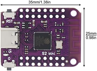
ESP32-S2 Mini Pinout: GPIO, USB OTG, and ADC

ESP32-S2 Mini development board with USB-C port and pin headers. Caption: ESP32-S2 Mini board, front view with USB-C port. Description: Top view of the ESP32-S2 Mini board used in this pinout guide.

ESP32-S2 Mini Pinout Guide: GPIO, USB OTG, and ADC

The ESP32-S2 Mini pinout starts with one clear limit: this chip has WiFi only, and it has no Bluetooth. The ESP32-S2 chip has 43 GPIO pins. It runs a single-core Xtensa LX7 core at 240 MHz. Native USB OTG uses GPIO19 and GPIO20. DAC uses GPIO17 and GPIO18.

Quick facts

Item Value Source
Chip GPIO count 43 GPIO pins ESP32-S2 Series Datasheet
Core Single-core Xtensa LX7 at 240 MHz ESP32-S2 Series Datasheet
Radios WiFi only, no Bluetooth ESP32-S2 Series Datasheet
Logic voltage 3.3 volts ESP32-S2 Series Datasheet
USB OTG pins GPIO19 D- and GPIO20 D+ ESP32-S2 Series Datasheet
ADC1 pins GPIO1 to GPIO10 ESP32-S2 Series Datasheet
ADC2 pins GPIO11 to GPIO20 ESP32-S2 Series Datasheet
DAC pins GPIO17 and GPIO18 ESP32-S2 Series Datasheet
UART0 pins GPIO43 TX and GPIO44 RX ESP32-S2 Series Datasheet
Strapping pins GPIO0, GPIO45, GPIO46 ESP32-S2 Series Datasheet
Module GPIO count 37 GPIO pins on ESP32-S2-MINI-2 ESP32-S2-MINI-2 Datasheet v1.4
Module flash 4 MB flash, optional 2 MB PSRAM ESP32-S2-MINI-2 Datasheet v1.4

ESP32-S2 Mini pinout table

Use this table as the chip reference. Match each GPIO number to the silkscreen on your board before you wire it.

GPIO Main role Notes
GPIO0 Strapping and boot Hold low at reset for download mode
GPIO1 to GPIO10 ADC1 channels 0 to 9 Analog input, 3.3 volt max
GPIO11 to GPIO16 ADC2 channels 0 to 5 ADC2 shares use with WiFi
GPIO17 ADC2 channel 6, DAC channel 1 True analog output pin
GPIO18 ADC2 channel 7, DAC channel 2 True analog output pin
GPIO19 ADC2 channel 8, USB OTG D- Native USB, not an ADC pin in use
GPIO20 ADC2 channel 9, USB OTG D+ Native USB, not an ADC pin in use
GPIO21 to GPIO32 General GPIO Check board silkscreen for exposure
GPIO33 to GPIO42 General GPIO Check board silkscreen for exposure
GPIO43 UART0 TX Serial transmit pin
GPIO44 UART0 RX Serial receive pin
GPIO45 Strapping Check level at boot
GPIO46 Strapping Check level at boot

The header order on the LOLIN S2 Mini board follows the WEMOS S2 Mini schematic V1.0.0. Each side has two rows of 8 pins. J2 is the right outer row, J5 the right inner row, J4 the left inner row, and J3 the left outer row, with pin 1 at the top of each row in the schematic.

Header Pin order, top to bottom
J2, right outer EN, GPIO3, GPIO5, GPIO7, GPIO9, GPIO11, GPIO12, 3V3
J5, right inner GPIO1, GPIO2, GPIO4, GPIO6, GPIO8, GPIO10, GPIO13, GPIO14
J4, left inner GPIO40, GPIO38, GPIO36, GPIO34, GPIO21, GPIO17, GND, GPIO15
J3, left outer GPIO39, GPIO37, GPIO35, GPIO33, GPIO18, GPIO16, GND, VBUS

That is 27 GPIO pins on the headers in total. GPIO0 is not on the headers; it is the BOOT button only. GPIO15 carries the blue onboard LED. Check the silkscreen on your board against this table before you wire it.

Power pins

Power the board through the USB-C port at 5 volts. The board steps that input down to 3.3 volts for the chip through an ME6211C33 regulator, per the WEMOS S2 Mini schematic V1.0.0. The ME6211 is a 500 milliampere class LDO, so treat 500 milliamperes as the ceiling for the whole 3.3 volt rail, chip included, and keep external 3.3 volt loads well below it. Do not feed 5 volts into any GPIO pin. Use a short USB cable under 3 feet long for stable uploads. Power motors and servos from a separate supply, not from the board. Share a common ground between the board and that supply. Check the silkscreen for the 5 volt, 3.3 volt, and ground labels on your board.

Strapping and boot pins

Strapping pins set the boot mode at reset. The ESP32-S2 strapping pins are GPIO0, GPIO45, and GPIO46, per the ESP32-S2 Series Datasheet. GPIO0 low at reset enters download mode for flashing. GPIO0 high at reset starts the normal sketch. Do not tie a strapping pin hard to 3.3 volts or ground. Keep boot pins free during the first test. If the board will not boot, remove wires from GPIO0, GPIO45, and GPIO46 first. Then test the board with no wires attached.

ADC pins

ADC1 uses GPIO1 to GPIO10, per the ESP32-S2 Series Datasheet. Use ADC1 for analog sensors when WiFi is on. ADC2 uses GPIO11 to GPIO20, per the same datasheet. ADC2 does not work well while WiFi runs. Keep analog input at or below 3.3 volts. Use a voltage divider for a sensor that outputs more than 3.3 volts. Do not use GPIO19 and GPIO20 as ADC inputs, since they carry USB OTG.

DAC and touch pins

DAC uses GPIO17 and GPIO18, per the ESP32-S2 Series Datasheet v1.9. Those two pins give a true analog voltage output. Use them for a simple analog test or a low-speed analog signal. Touch uses GPIO1 to GPIO14, which are TOUCH1 to TOUCH14, per the ESP32-S2 Series Datasheet v1.9, section 2.3.4. All 14 touch pins double as ADC pins: GPIO1 to GPIO10 are ADC1, and GPIO11 to GPIO14 are ADC2 channels 0 to 3.

PWM pins

Most GPIO pins can output PWM through the LEDC driver in the Arduino core. Pick a free GPIO pin that is not a strapping pin, a USB pin, or a DAC pin. Use a 5,000 Hz frequency for an LED test. Use a 50 Hz frequency for a servo signal. Drive a motor through a driver board, never direct from a GPIO pin. See the ESP32 family comparison for how the S2 differs from the S3 on Bluetooth and USB.

I2C pins

I2C can use most GPIO pins on the ESP32-S2, per the ESP32-IDF GPIO reference. No fixed SDA and SCL pins are stated in the verified source data for this post. Pick two free GPIO pins and set them in code. Add pull-up resistors of 4.7 kilo-ohms to 3.3 volts on SDA and SCL if your sensor board lacks them. Keep I2C wires under 1 foot long where you can. Use 3.3 volt I2C sensors only. For the I2C protocol behind the wiring, see I2C vs SPI vs UART: Which Protocol for Your Sensor or Display.

SPI pins

SPI can also use most GPIO pins on the ESP32-S2, per the ESP32-IDF GPIO reference. No fixed MOSI, MISO, SCK, and CS pins are stated in the verified source data for this post. Pick free GPIO pins and set them in code. Use one CS pin per SPI device. Start at a low clock speed, such as 1,000,000 Hz. Use 3.3 volt SPI devices only.

UART pins

UART0 uses GPIO43 for TX and GPIO44 for RX, per the ESP32-S2 Series Datasheet. UART0 is the main serial port for debug output. A second UART can use other free GPIO pins in code. Keep UART wires crossed: TX on one board goes to RX on the other board. Use 3.3 volt UART signals only. Set both ends to the same baud rate, such as 115,200 baud.

USB pins

Native USB OTG uses GPIO19 for D- and GPIO20 for D+, per the ESP32-S2 Series Datasheet. The S2 Mini board brings these pins to a USB-C port. Use that port for flashing and for serial output. Do not use GPIO19 or GPIO20 for sensors. Use a data-capable USB cable, not a charge-only cable. Use a cable under 3 feet long for uploads. USB OTG lets the board act as a USB host for some devices, but that needs host code. The pin test sketch below uses the port for serial only.

Pins to avoid

Avoid GPIO0, GPIO45, and GPIO46 for sensors that pull the pin low at boot. Avoid GPIO19 and GPIO20 for sensors, since they carry USB OTG. Avoid ADC2 pins GPIO11 to GPIO20 for analog reads while WiFi is on. Avoid GPIO17 and GPIO18 for digital loads if you need DAC output. Avoid 5 volt signals on every GPIO pin. The chip uses 3.3 volt logic only. If a pin is not on the board silkscreen, leave it alone and pick an exposed GPIO pin instead.

Max current and logic voltage

Logic voltage is 3.3 volts on all GPIO pins, per the ESP32-S2 Series Datasheet v1.9. At the strongest drive setting, a GPIO pin sources about 40 mA (IOH) and sinks about 28 mA (IOL), per Table 5-4 of the same datasheet. Those are drive-strength values at 3.3 volts, not a recommended continuous load, and the default drive strength is 20 mA. Treat a small LED through a resistor as the practical per-pin load, not 40 mA. Drive a relay, a motor, or a servo through a driver or a transistor. The 3.3 volt rail ceiling is 500 milliamperes from the ME6211C33 regulator, per the WEMOS S2 Mini schematic V1.0.0.

Wiring and power warnings

Check the voltage of every sensor before you wire it. A 5 volt sensor output can harm a 3.3 volt GPIO pin. Remove power before you move wires. Do not short the 3.3 volt pin to ground. If the board smells hot, unplug it at once. Use a separate supply for motors and servos. Share only the ground wire between supplies. Keep the board on a non-metal surface while you test it.

Pin test sketch

This sketch blinks an external LED on GPIO4 and reads ADC1 on GPIO1. It uses only the Arduino core for ESP32, version 3.3.13. No extra library is needed. Wire the LED anode to GPIO4 through a 220 ohm resistor. Wire the LED cathode to ground. Wire a potentiometer wiper to GPIO1. Code status: code not compiled. No Arduino CLI or PlatformIO is installed here, so compilation was not run.

// ESP32-S2 Mini pin test sketch
// Board: ESP32-S2 Mini, Arduino core for ESP32 version 3.3.13
// Code status: code not compiled
// LED on GPIO4, ADC input on GPIO1, serial at 115200 baud
const int ledPin = 4; // GPIO4, plain digital pin
const int adcPin = 1; // GPIO1, ADC1 channel 0
void setup() {
  Serial.begin(115200); // Start serial for test output
  pinMode(ledPin, OUTPUT); // Set LED pin as output
  delay(500); // Wait 500 ms for serial to settle
}
void loop() {
  digitalWrite(ledPin, HIGH); // Turn LED on
  int adcValue = analogRead(adcPin); // Read ADC1 on GPIO1
  Serial.print("ADC1 GPIO1 value: "); // Label the reading
  Serial.println(adcValue); // Print raw ADC count
  delay(500); // Wait 500 ms with LED on
  digitalWrite(ledPin, LOW); // Turn LED off
  delay(500); // Wait 500 ms with LED off
}

If the LED blinks and the serial monitor shows ADC values that change with the potentiometer, GPIO4 and GPIO1 both work. If the LED stays dark, check the resistor value and the LED polarity. If the ADC value stays at 0, check the potentiometer wiring to GPIO1.

Frequently asked questions

Does the ESP32-S2 Mini have Bluetooth?

No, the ESP32-S2 chip has WiFi only and no Bluetooth, per the ESP32-S2 Series Datasheet. Do not use Bluetooth code on this board. Use WiFi or USB for a wireless link instead.

Which pins are safe for a first sensor on the ESP32-S2 Mini?

Use ADC1 pins GPIO1 to GPIO10 for analog sensors, per the ESP32-S2 Series Datasheet. Use GPIO4 for a plain digital test. Keep strapping pins, USB pins, and DAC pins free unless you need them.

Can the ESP32-S2 Mini use 5 volt sensors?

No, the GPIO pins use 3.3 volt logic only, per the ESP32-S2 Series Datasheet. A 5 volt signal can harm a GPIO pin. Use a level shifter or a voltage divider for a 5 volt sensor.

Why does my board fail to boot after I add wiring?

A strapping pin may be held low at reset. The strapping pins are GPIO0, GPIO45, and GPIO46, per the ESP32-S2 Series Datasheet. Remove wires from those pins and test the board with no wires attached.

Why does ADC2 read poorly when WiFi is on?

ADC2 shares hardware with WiFi on the ESP32-S2, per the ESP32-S2 Series Datasheet. ADC2 uses GPIO11 to GPIO20. Use ADC1 pins GPIO1 to GPIO10 for reads while WiFi runs.

Can I use GPIO19 and GPIO20 for a sensor?

No, GPIO19 and GPIO20 carry native USB OTG on this board, per the ESP32-S2 Series Datasheet. Use them only for USB. Pick a different free GPIO pin for the sensor.

Product callout

Start with the ESP32-S2 Mini Development Board for a first board at the bench. For a single spare, see the ESP32-S2 Mini Development Board Single. For a bench stock of boards, see the ESP32-S2 Mini Development Board 10-Pack. Check stock on the product page at order time.

Sources

Last updated: 2026-11-21. Status: STAGED ONLY, zero live writes, zero publishes.